I’m currently reading the Computer Architecture: A quantitative approach book and after so many diagrams that are connected, but that never appear together I decided to summarize everything in a design. It’s not intended to be complete, as there are many ways of solving this topic, but from a hypothetical perspective it gives a good perspective on how memory mapping works in current computer architecture.
Introduction
This post examines the memory mapping flow within a hypothetical 64-bit computer architecture. The system employs a three-level cache hierarchy, starting with a Translation Lookaside Buffer (TLB) for virtual-to-physical address translation. Subsequent levels include a 32KB L1 cache (organized into 256 sets with 2-way associativity and 512-bit block size) and a 4MB L2 cache (comprising 16,384 sets with 4-way associativity and 512-bit block size). For the purpose of illustrating the mapping process, we’ll present a simplified model that combines instruction and data caches. We will not discuss block replacement algorithms or write-back mechanisms in this post.
How memory mapping works?
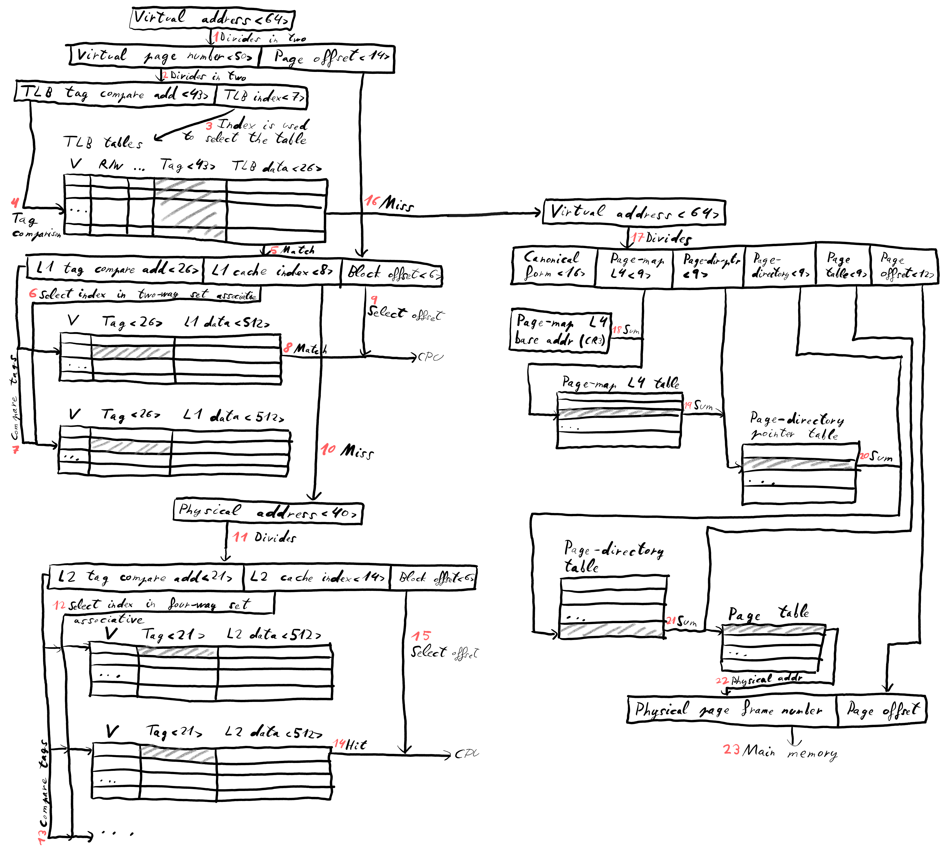 | Visual explanation of the memory mapping process |
Numbers in red explain how the diagram should be read and each one explains the following:
- The virtual address is divided into two parts: virtual page number and page offset.
- The virtual page number is divided in two parts: TLB tag compare address and TLB index.
- The TLB uses the TLB index to look up the corresponding entry in the tables.
- The TLB tag is compared with the tag stored in the TLB entry.
- TLB hit.
- The L1 cache index is used to select the set in the cache.
- The L1 cache tag is compared with the tag stored in the L1 cache entry.
- L1 cache hit.
- The block offset selects the offset from L1 data and this is sent to the CPU.
- L1 cache miss.
- Let’s take back the physical address and divide it in: L2 tag compare address, L2 cache index and block offset.
- The L2 cache index is used to select the set in the cache.
- The L2 cache tag is compared with the tag stored in the L2 cache entry.
- L2 cache hit.
- The block offset selects the offset from L2 data and this is sent to the CPU.
- Let’s come back to the TLB cache miss.
- The virtual address is divided in: canonical form, page-map L4 entry, page-directory-pointer entry, page directory entry, page table entry and page offset.
- The CR3 register entry is summed to the page-map L4 to obtain the location of the page-directory-pointer table.
- The page-directory-pointer table is summed to the page-directory-pointer entry to obtain the location of the page directory table.
- The page directory table is summed to the page directory entry to obtain the location of the page table entry.
- The page table is summed to the page table entry to obtain the physical address.
- The physical address is the physical page frame number.
- The physical page frame number and the page offset indicate the exact location in main memory.
Conclusion
I enjoyed understanding and explaining the memory mapping process in this hypothetical architecture. I hope you found it helpful and that it demystified some of the inner workings of computer memory. Thanks for reading!