I continue my reading of Computer Architecture: A quantitative approach and there was something that caught my eye and that I’d like to expand the explanation: how DRAM memory banks work.
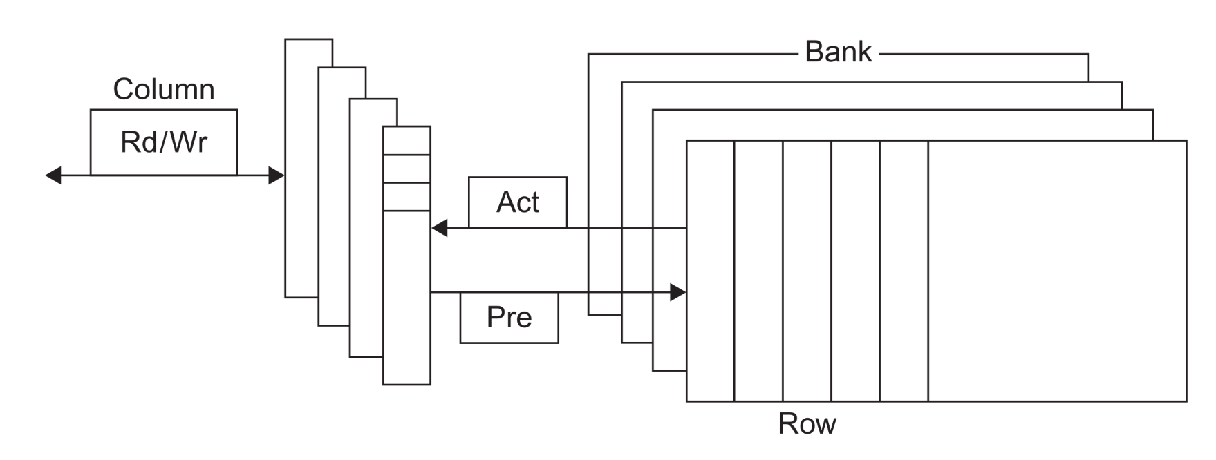 | Internal organization of a DRAM from Computer Architecture: A quantitative approach |
The image is a simplified visual representation of a DRAM chip’s internal structure. Here’s what each part represents:
- Bank: think of banks as independent memory units within the DRAM chip. Modern DRAMs have multiple banks (up to 16 in DDR4), allowing for parallel operations and increased efficiency.
- Row: rach bank is divided into rows, like rows in a spreadsheet. A row is a large collection of memory cells.
- Column: when a row is activated, the data within it is accessed by columns. Think of columns as individual cells within a row.
- Rd/Wr: this represents the Read/Write operation. Data can be read from or written to the selected column.
- Act (Activate): this command opens a specific bank and row, copying the data from the row into a temporary storage area called the row buffer.
- Pre (Precharge): this command closes the currently open bank and row. It essentially resets the bank, preparing it for a new access.
Key concepts explained
Let’s redesign the previous image as a sequence diagram to break down the DRAM operation:
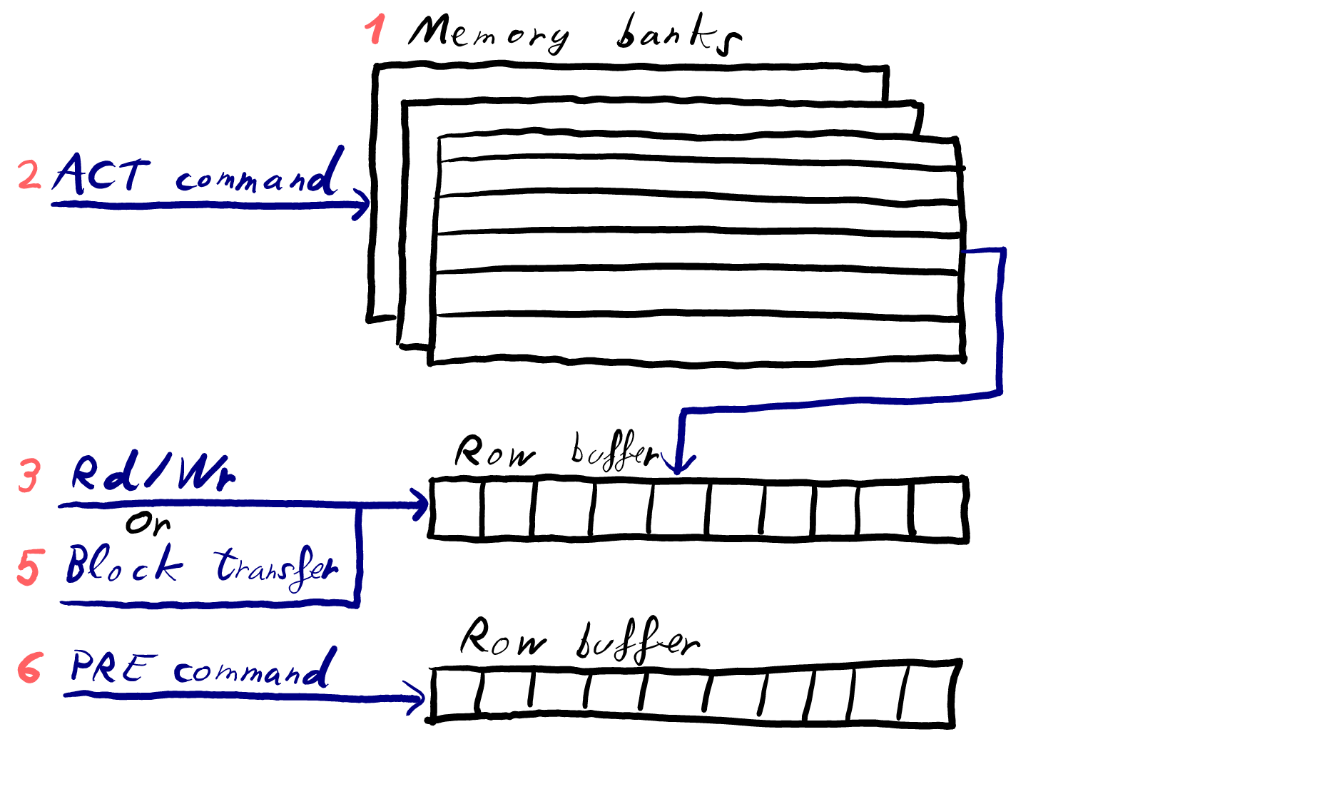 | DRAM sequence diagram |
- Banks for parallelism: the multiple banks are crucial for performance. By having independent banks, the memory controller can issue commands to different banks simultaneously, improving data throughput.
- Row activation (ACT): the ACT command initiates the process of accessing a specific row within a DRAM bank. When the memory controller issues an ACT command, it provides the bank and row address. This triggers the DRAM to copy the entire contents of the selected row into a temporary storage area called the row buffer. This is a critical performance optimization, as accessing data within the row buffer is significantly faster compared to directly accessing the individual memory cells. This speed difference stems from the fact that the row buffer is designed for rapid access, while the memory cells themselves are optimized for density and storage capacity.
- Column access (Rd/Wr): once the row is in the buffer, you can read or write data to specific columns within that row using the Rd/Wr signals.
- Data transfer width: this refers to how many bits of data are transferred at a time. A wider transfer width means more data can be moved in a single cycle, increasing bandwidth.
- Block transfers: instead of accessing individual columns one by one, you can perform block transfers. This means reading or writing a contiguous block of data starting from a specific address, further improving performance by reducing command overhead and improving cache line fills.
- Precharge (PRE): after you’re done accessing data in a row, you need to close it with the PRE command. It prepares the bank for the next ACT command.
- Clock synchronization: all these operations are synchronized with a clock signal. This ensures that the memory controller and DRAM work together in a coordinated manner. The clock frequency directly influences DRAM bandwidth.
In simpler terms
Think of a DRAM as a large library with multiple rooms (banks). Each room has shelves (rows) with books (data). To access a book, you first need to open the correct room and pull the entire shelf into a reading area (row buffer). Then, you can pick the specific book you need. When you’re done, you return the shelf and close the room.